|
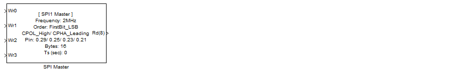
<< Click to Display Table of Contents >> SPI Master |
  
|
|
<< Click to Display Table of Contents >> SPI Master |
|
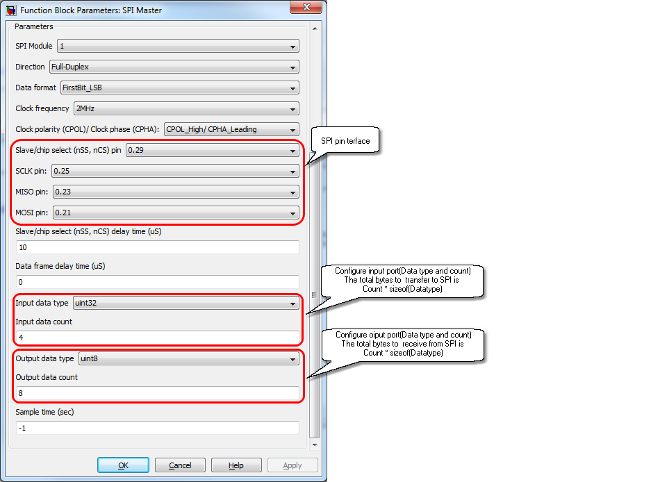
Configuration item |
Selectable option/ Value |
Description |
|---|---|---|
SPI Module |
0 | 1 |
|
Direction |
Full-Duplex | Half-Duplex_Tx | Half-Duplex_Rx |
Full-Duplex: MISO, MOSI and clk available for communication. Half-Duplex_Tx: MOSI and clk available for communication. Half-Duplex_Rx: MISO and clk available for communication. |
Data format |
FirstBit_MSB | FirstBit_LSB |
FirstBit_MSB: the first bit of receiving byte is MSB. FirstBit_LSB: the first bit of receiving byte is LSB. |
Clock frequency |
125kHz | 250kHz | 500kHz | 1MHz | 2MHz |4MHz |
SPI clock frequency selection. |
Clock polarity (CPOL)/ Clock phase (CPHA): |
CPOL_Low/ CPHA_Leading | CPOL_Low/ CPHA_Trailing | CPOL_High/ CPHA_Leading | CPOL_High/ CPHA_Trailing |
CPOL_Low/ CPHA_Leading: clock polarity LOW and capture on leading (1st) edge. CPOL_Low/ CPHA_Trailing: clock polarity LOW and capture on trailing (2nd) edge. CPOL_High/ CPHA_Leading: clock polarity HIGH and capture on leading (1st) edge. CPOL_High/ CPHA_Trailing: clock polarity HIGH and capture on trailing (2nd) edge. |
Slave/chip select (nSS, nCS) pin |
Select GPIO pin for CSS or "None" if this SPI pin did not controlled by this block. |
|
SCLK pin: |
Select GPIO for SPI clock. |
|
MISO pin: |
Select GPIO pin for MISO. |
|
MOSI pin: |
Select GPIO pin for MOSI. |
|
Slave/chip select (nSS, nCS) delay time (uS) |
Optional, in the case that need some delay to after CSS pin activate. The delay value is in seconds.. |
Delay time in uS, between the falling edge of CSS and the first byte of data in a transaction. |
Data frame delay time (uS) |
Optional, in the case that need more delay time beterrn bytes. |
|
Sample timer (sec) |
(Specify block sample time) |