|
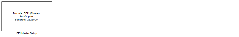
<< Click to Display Table of Contents >> SPI Master Setup |
  
|
|
<< Click to Display Table of Contents >> SPI Master Setup |
|
Configuration item |
Selectable option/ Value |
Description |
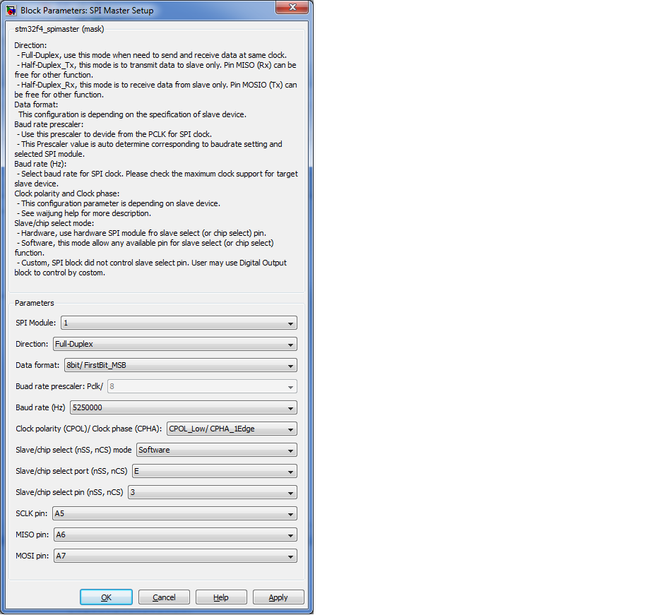
SPI Module |
1 | 2 | 3 |
Specify using SPI module for setup/ configuration. |
Direction |
Full-Duplex | Half-Duplex_Tx | Half-Duplex_Rx |
Full-Duplex: use this mode when need to send and receive data at same clock. Half-Duplex_Tx: this mode is to transmit data to slave only. Pin MISO (Rx) can be free for other function. Half-Duplex_Rx: this mode is to receive data from slave only. Pin MOSIO (Tx) can be free for other function. |
Data format |
8bit/FirstBit_MSB | 8bit/FirstBit_LSB | 16bit/FirstBit_MSB | 16bit/FirstBit_LSB |
Specify data format. Must be match to the slave device specification. |
Baud rate prescaler |
2 | 4 | 8 | 16 | 32 | 64 | 128 | 256 |
This configuration related to SPI clock speed. |
Baud rate (Hz) |
(Select SPI clock speed) |
This clock speed depending on SPI module. For example: SPI1: clock source is PCLK2, 84MHz (max). For prescaler 2, 4, ..., 256 SPI clock speed can be: 42MHz, 21MHz, 10.5MHz, 5.25MHz, 2.625MHz, 1.3125MHz, 0.65625MHz and 0.328125MHz respectively. SPI2 and SPI3: clock source is 42MHz (max). SPI clock can be: 21MHz, 10.5MHz, ... respectively. |
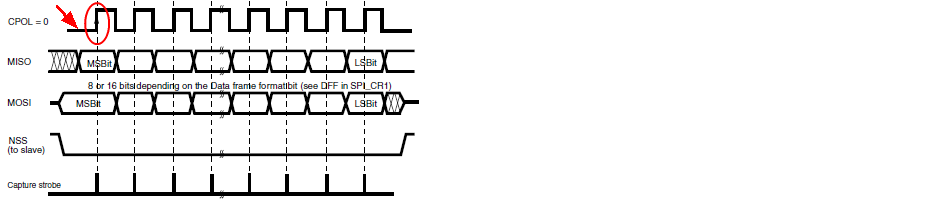
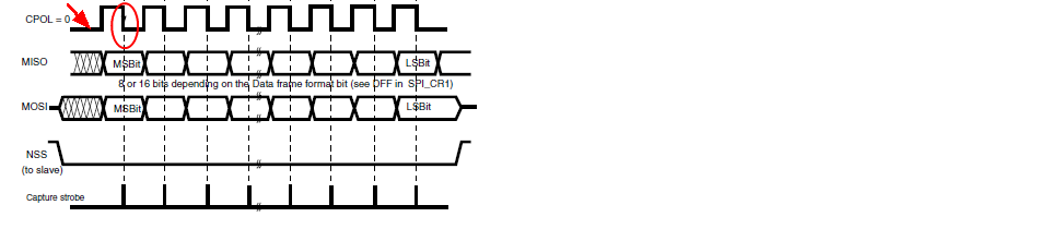
Clock polarity (CPOL)/ Clock phase (CPHA) |
CPOL_Low/ CPHA_1Edge | CPOL_Low/ CPHA_2Edge | CPOL_High/ CPHA_1Edge | CPOL_High/ CPHA_2Edge |
Clock polarity and clock phase configuration, must be matched to SPI slave/device. |
Slave/chip select mode |
Software | Hardware | Custom |
Select NSS control signal is by hardware or software (manual). |
Soft slave/chip select port |
A | B | C | D | E | F | G | H | I |
Select port for software NSS, this configuration available when NSS mode is Software. |
Soft slave/chip select pin |
0 | 1 | 2 | 3 | 4 | 5 | 6 | 7 | 8 | 9 | 10 | 11 | 12 | 13 | 14 | 15 |
Select pin for software NSS, this configuration available when NSS mode is Software. |
Slave/chip select pin |
(Depending on MCU package pin) |
Select pin for NSS for using NSS hardware mode. |
SCLK pin |
(Depending on MCU package pin) |
Select pin for SCLK. |
MISO pin |
(Depending on MCU package pin) |
Select pin for MISO. |
MOSI pin |
(Depending on MCU package pin) |
Select pin for MOSI. |
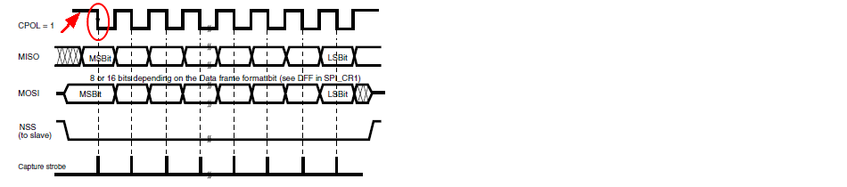
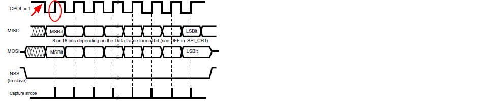
This clock configuration to capture a valid data, must be follow to slave device specification.
This configuration for data bit captured at first edge of Clock. First edge of clock is rising.
CPOL=0 and CPHA=0
This configuration for data bit captured at second edge of Clock. Second edge of clock is falling.
CPOL=0 and CPHA=1
This configuration for data bit captured at first edge of Clock. First edge of clock is falling.
CPOL=1 and CPHA=0
This configuration for data bit captured at second edge of Clock. second edge of clock is rising.
CPOL=1 and CPHA=0
Pin name |
Alternative naming |
Function |
SCLK |
SCK, CLK, CK |
Serial clock output, from master to slave. |
MOSI |
MDO, SDO, DO |
Serial data output, from master to slave. |
MISO |
MDI, SDI, DI |
Serial data input, from slave to master. |
NSS |
CS, nCS |
Slave select or chip select pin. |