|
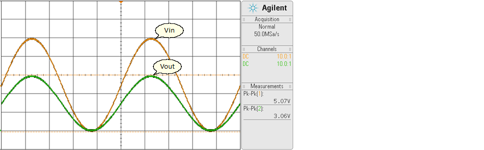
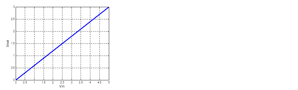
<< Click to Display Table of Contents >> Vin = 0 – 5 V, Vout = 0 – 3 V |
  
|
|
<< Click to Display Table of Contents >> Vin = 0 – 5 V, Vout = 0 – 3 V |
|
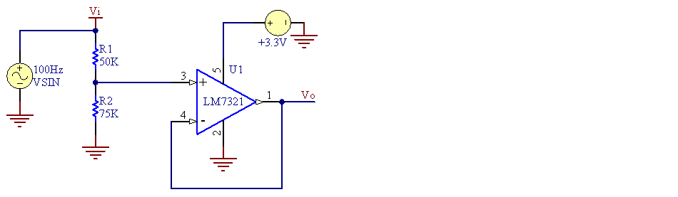
The non-inverting attenuation can be performed with a voltage divider and a buffer circuit. The voltage divider circuit, R1 and R2 use to reduce the input voltage form 5 V to 3 V. The value of resistor can calculate by:
Example
Vo = VR2 (+ input pin)
VR2 = Vi ×R2/(R1+R2)
Give R2 = 75 kΩ, Vi = 5 V, Vo = 3 V
R1 = ((Vi ×R2)/VR2)-R2
= ((5V ×75kΩ)/3V)-75kΩ
= 50kΩ
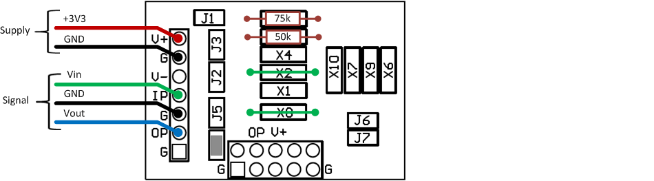
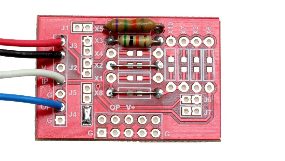
Configuration of aMG SIGCON-A: Soldering to Jump J4, X2, and X8. Place 50 kΩ resistor to X3, and 75 kΩ to X5.