|
<< Click to Display Table of Contents >> Vin 0-3 V, Vout -12 to +12 V |
  
|
|
<< Click to Display Table of Contents >> Vin 0-3 V, Vout -12 to +12 V |
|
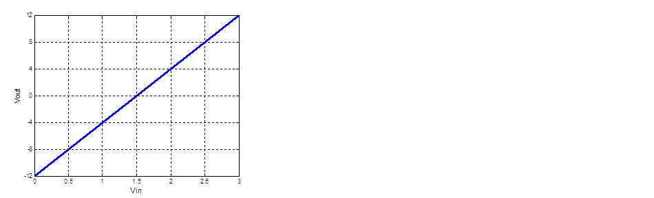
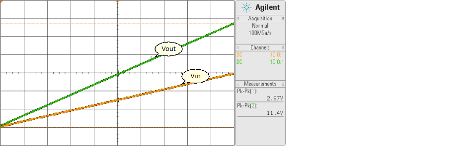
The set of data points, Vout = -12 V @ Vin = 0 V, Vout = +12 V @ Vin = +3 V, see the transfer curve below.
-12 = m(0) + b
12 = m(3) + b
After algebraic manipulation, yield the solution, m = 8 and b = -12, rewrite m and b to new equation.
Vout = 8Vin - 12
The equation above similar to the CASE2: Vout = +mVin - b circuit.
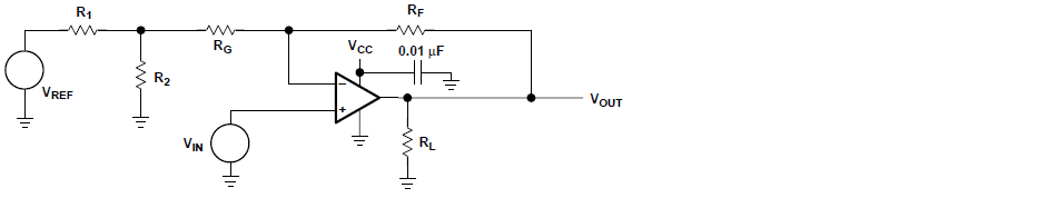
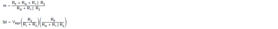
We can calculate the value of R1, R2, RF and RG by the following equations:
The circuit configuration which yields a solution is shown below.
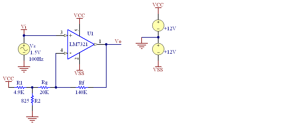
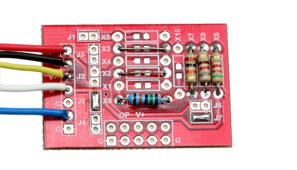
Configuration of aMG SIGCON-A: Soldering to Jump J5, J7, X2 and X3. Place 5 kΩ resistor to X6, 20 kΩ to X7, 150 kΩ to X8 and 820 Ω to X9 .
The recommended design procedure for zero-span op-amp design is:
| 1. | Substitute the data set into linear equations to obtain m and b (the slope and intercept of a straight line). |
| 2. | Determine the form of the circuit by m and b then choose the circuit configuration that fits the form. |
| 3. | Using the circuit equations which selected, calculate the resistor values. |
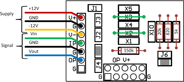
| 4. | Build the circuit using aMG SIGCON-A. |
| 5. | Test the circuit, take data and verification. |