|
<< Click to Display Table of Contents >> Voltage Follower |
  
|
|
<< Click to Display Table of Contents >> Voltage Follower |
|
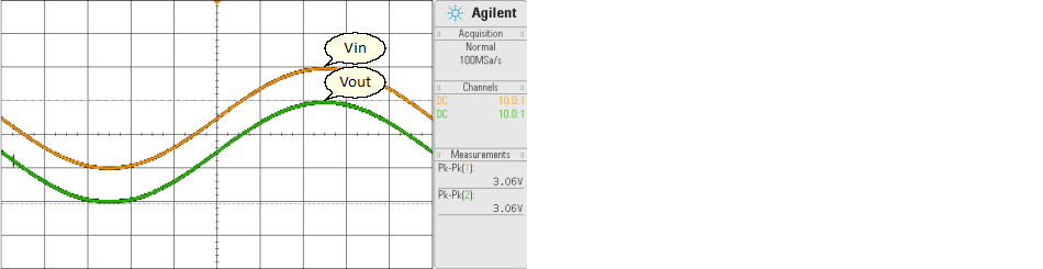
The voltage follower circuit’s gain is 1. Sometime it was called a unity gain amplifier, buffer amplifier, it may be constructed simply by connecting its output to its inverting input, and connecting the signal source to the non-inverting input. This connection forces the op-amp to adjust its output voltage simply equal to the input voltage (Vo follows Vi), so the circuit is named voltage follower.
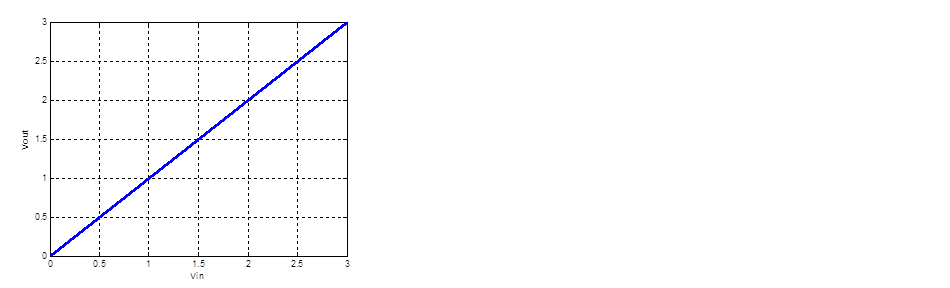
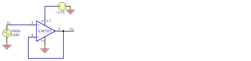
Vo = Vi
The importance of this circuit come from the input and output impedance of the op-amp. The input impedance of the op-amp is very high (1 MΩ to 10 TΩ), meaning that the input of the op-amp does not load down the source and draws only minimal current from it. Because the output impedance of the op-amp is very low, it drives the load as if it were a perfect voltage source. Both the connections to and from the buffer are therefore bridging connections, which reduce power consumption in the source, distortion from overloading, crosstalk and other electromagnetic interference.
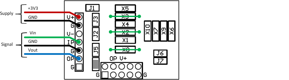
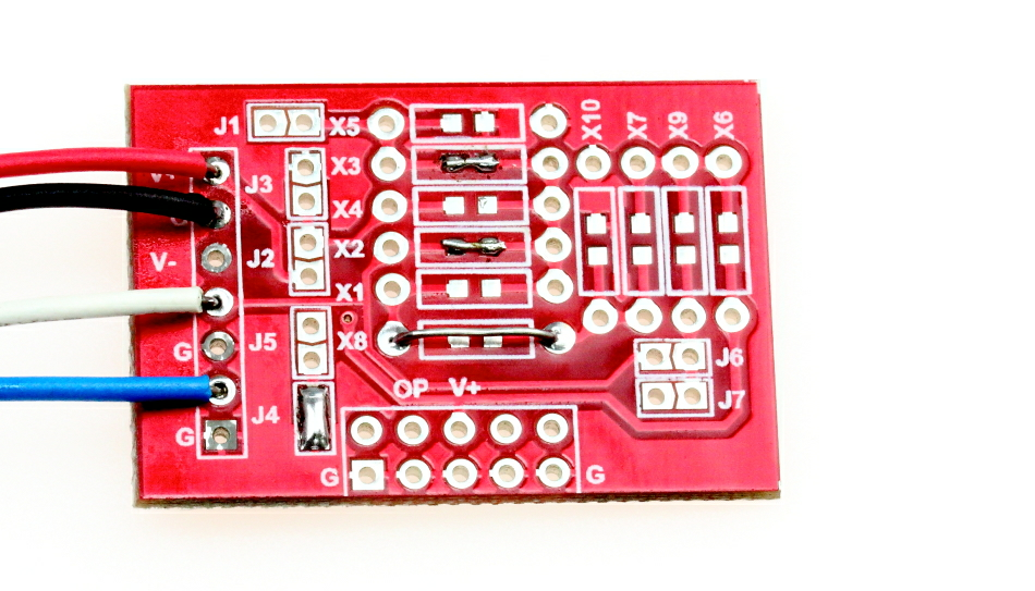
Using aMG SIGCON-A as the Voltage Follower Circuit: Soldering to Jump J4, X2, X3, X8 on a board.